The unseen in the center of an electronic gadget you use most of the day is the PCB board layout design. Without printed circuit boards that were expertly constructed, your smartphone, laptop, car, and coffee machine, to name just a few, would be useless. This is a pivotal step process that converts electrical schematics into real-life boards that energize our digital world.
Knowledge of PCB layout design enables engineers to develop superior products. It is less expensive and increases reliability. This guide will learn all about the PCB board layout design, including its pitfalls and related advanced topics.
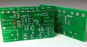
What Is PCB Board Layout Design?
Copper traces are designed by the designers who interconnect these components. How the signals move within the circuit is dependent on the layout.
It is like mapmaking electricity. All the parts require the appropriate linking. All the paths should ensure no interference with the signals. This is the work of the designer to achieve this effectively. Weak design causes signal interference, overheating, and part failures. When good design is used, it works effectively over a long period of years.
Key Components of PCB Layout
Electronic Components
Contemporary PCBs will have different components playing a range of functions:
- Electrical current is regulated with the help of resistors. They give particular resistance figures in ohms. Resistors prevent an inordinate amount of current from damaging sensitive components.
- Capacitors enclose and discharge electrical energy.
- The various kinds cover various areas of frequency.
- Integrated circuits carry out elaborate activities. These small computers deal with anything as basic as logic or on a higher level of processing. ICs usually define the chief task of the board.
The PCB is connected with other external devices using connectors. They give input of power and signal connections. The right position of connectors influences assembly and production.
Traces and Layers of Copper Traces
Electrical pathways between components are with copper traces. Current-carrying capacity is dependent on trace width.
Modern PCBs use multiple layers. Signal layers carry data between components. Power layers distribute electricity efficiently. Ground layers provide electrical reference points.
The layer stack-up affects signal integrity. Proper spacing prevents electrical interference. Layer count impacts manufacturing costs significantly.
The PCB Layout Design Process
The PCB Layout Design process is as follows:
- Step 1: Schematic Analysis
- Step 2: Component Placement
- Step 3: Routing and Trace Design
- Step 4: Design Rule Checking
Common PCB Layout Design Challenges
Space Constraints
The demands of modern electronics require miniaturization. Miniaturization of components is still taking place. The density of the layout creates a challenge in manufacturing. The many-layer boards are more densely functional. Via-in pad saves space. Microvias make it possible to run ultra-dense connections.
Signal Interference
Electromagnetic interference occurs on sensitive circuits. Effective shielding methods curtail the problems. The ground plane design removes the crosstalk. Analog signals are polluted by power supply noise. Power plane design applies clean power on a wide basis.
Manufacturing Limitations
Designs are constrained by fabrication possibilities. A minimum trace width is vendor-dependent. Through sizes influence the cost of drilling. The component selection is affected by assembly constraints. Pick and place machines are limited in accuracy. Fine-pitch components are highly sensitive. The PCB layout is a critical business process where a variety of best practices can be deployed to support success.
Planning Phase
Proper planning eliminates the redesigns, which are expensive. The choice of components can influence the complexity of the layout. Supplier involvement early characterizes the problems.
The stack-up planning maximizes signal routing. The number of layers is a compromise between price and performance. Decisions are made using contact with manufacturing partners.
Design Execution
Formal routing strategies are most successful. High priority is given to critical signals. Records are kept of design decisions. The early detection of errors is through design reviews.
Verification Steps
Several slots of verification are granted. Electrical rule checking accepts links. The manufacturability is checked by physical design rules.
Validation on the design is by prototype testing. Problems in the early stages are detected early. Performance is improved through an iterative process.
Advanced PCB Layout Techniques
High-Speed Design
Special techniques are needed in high-speed circuits. Controlled impedance routing preserves the signal integrity. Timing is accomplished through length matching. Noise sensitivity is decreased. Further isolation is in guard traces. Through optimization, discontinuities are reduced.
RF and Microwave Design
Special consideration should be made for radio frequency circuits. When choosing the routing paths, transmission line theory is used. Performance is sensitive to how it is designed as a ground plane. RF principles are used in the placement of components. Unwanted coupling is avoided by isolation. Shielding comprises electromagnetic energy.
Flex and Rigid-Flex PCBs
New form factors can be enabled by the use of flexible circuits. Failures are avoided with bend radius calculations. Special materials are needed for dynamic flexing.
Rigid-flex is a merger of both technologies. The areas in in-between should be thoughtfully designed.
Future Trends in PCB Layout Design
Artificial Intelligence Integration
To place the components optimum use of AI tools is used. Routing efficiency is better with machine learning. Design rule verification is faster with automation. The predictive analysis finds possible failures. Optimization algorithms of the design enhance performance. Human models are still needed.
Advanced Materials
Increasing frequencies are made possible because of new substrate materials. Signal integrity is enhanced by dielectrics that have low losses. There is better management of heat by the Thermal interface material. Processing power is incorporated in active substrates. The manufacturing process keeps changing.
Environmental Considerations
Lead-free soldering impacts the material choice of the components. Material selection is impelled by RoHS compliance. Design choices are made based on recycling.
Energy efficiency is becoming more significant. Power management circuits cut down power use. There is uptake of green manufacturing processes.
Conclusion
The design of the PCB board is the way forward in our technology. All an electronic invention begins with a well-engineered board of circuitry,the product of skilled pcb design and layout services.The engineering field is a branch of electrical engineering and physics, as well as manufacturing. The world today is built on dependable electronics. The designs that eliminate faults are required in autonomous cars. Medical equipment requires life-dependent reliability. Aerospace use cases go to extremes of performance.
The role of the layout designer keeps growing. More sophisticated simulation tools can produce insights. Reduced-size/speed designs are possible due to manufacturing capabilities. Practices of sustainability are motivated by environmental limitations. Learning is constant to succeed. The development of technology requires skill-building. Cross-disciplinary cooperation is a necessity. People measure success by quality.
The bridge between concept and reality is direly to be followed by PCB board design. Design work takes theoretical circuits into practical products. Electronics have a promising future with the aid of the cadre of skilled layout engineers that bring the ideas of their hands to the tools that run our world.
Source: FG Newswire